Processing Problems
Initial experiments and difficulties
Below are the pictures of some of our processed wafers. These wafers have
originally these specifications, and films deposi
ted.
Here is the processing steps:
Aluminum Etch
Type of etch: Wet Isotropic Etch
Chemical used: Transene Type APre-mixed Aluminum Etch
Machine used: None
Temperature of etch: Room Temperature
Advertised etch rate: 10 Angstroms/minute
Etch time: 9.5 minutes
Titanium/Tungsten Etch
Type of etch: Wet Isotropic Etch
Chemical used: Hydrogen Peroxide
Machine used: None
Temperature of etch: 100 Degrees C
Advertised etch rate: 150 Angstroms/minute
Etch time: 3 minutes
Silicon Dioxide Etch
Type of etch: Reactive Ion Etch (Anisotropic)
Chemical used: Trifluoromethane (CHF3) and Oxygen
Machine used: PlasmaTherm 790 RIE
Temperature of etch: In Plasma
Advertised etch rate: 0.3 microns/minute
Etch time: 60 minutes
Silicon Etch
Type of etch: Dry etch (anisotropic)
Chemical used: Trifluoromethane (CHF3) and oxygen
Machine used: XactixXetch Xenon Difluoride Etcher
Temperature of etch: Room Temperature
Advertised etch rate: 1 microns/minute
Etch time: 15 minutes
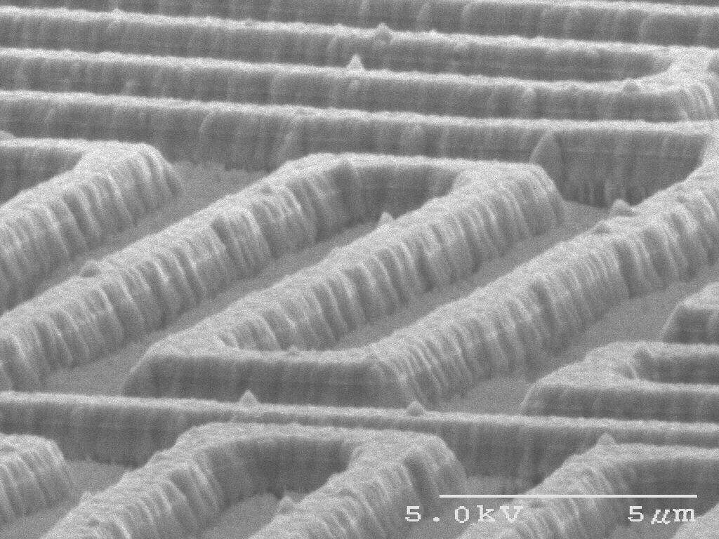
Here are the pictures. The idea is to use the metal layer as a mask for
both our silicon dioxide and silicon etching. As you can see, there is
this "stuff" that is deposited between the patterned areas. I
strongly believe this is the mask eroding according to literature I
read.(Click on the pictures to enlarge)

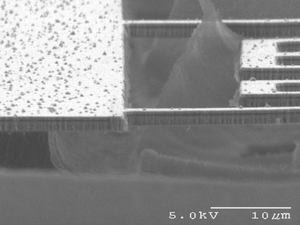
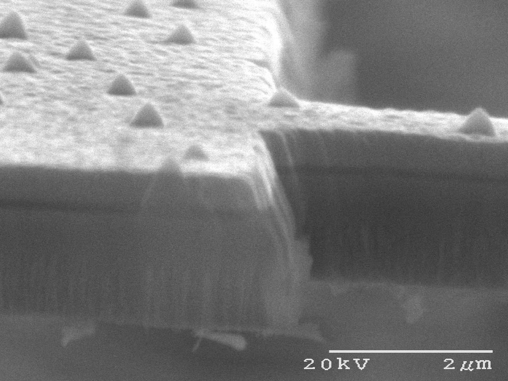
The wafers below received a different processing sequence, now we get this fine "mesh-like" structure forming between the paterned metal areas. Below is supposed to be a 300 micron wide by 100 micron deep trench into silicon. Unfortunately there is somet
hing still covering the trench and now we get these "grass-like" structures on the bottom of the trench, which I believe is caused from the masking caused by this "mesh-like" structure covering the trench.