Chemically-Assembled Electronic Nanotechnology
Chemically Assembled Electronic Nanotechnology (CAEN) is a form
of electronic nanotechnology which uses self-alignment to construct
electronic circuits out of nanometer-scale devices that take advantage of
quantum-mechanical effects. CAEN can be harnessed to create useful
computational devices with more than 1010 gate-equivalents per
cm2.
Chemists and physicists already have assembled molecular-scale
electronic devices and, everyday, research is producing new ones, with
better
properties.

Researchers have
also devised an electrical switch which can be built from a single
molecule. This switch can be configured (opened/closed) by applying a high
electric field, outside the normal operating range. It stores the
configuration for a relatively long time (minutes). In the conducive state
it behaves like a
diode.
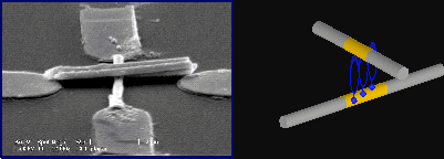
It is possible to cross nanowires and place configurable switches
at the junctions.
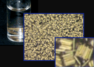
Large quantities of molecular wires and switches can be
inexpensively created using the process of self-assembly.
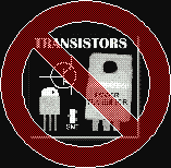
The Holy Grail of electronic nanotechnology today is the
manufacturing of transistors on a large scale. We claim that such an
effort is futile: even if transistors can, and have been built at the
nanoscale, it is virtually impossible to connect them with wires: at the
nanoscale the required alignment simply cannot be obtained using a
massively parallel fabrication technology.
Nanotechnology
on large scale offers us only two-terminal devices.
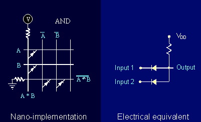
By using complementary logic and only diodes and resistors it is
possible to implement a set of complete logical functions. This example
shows the implementation of an and gate using diode-resistor
logic.
To obtain signal
amplification and clocking, our research group has devised a molecular
latch which can be built at the nanoscale using only two-terminal
devices.
  Unlike CMOS, CAEN is extremely unlikely to be
used to construct complex aperiodic structures. We introduce an
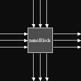
architecture based on fabricating dense regular structures, which we call
nanoBlocks, that can be programmed after fabrication to implement complex
functions. In our proposal nanoBlocks implement three-input to
three-output logic functions. We call an array of connected nanoBlocks a
nanoFabric. Unlike CMOS, CAEN is extremely unlikely to be
used to construct complex aperiodic structures. We introduce an
architecture based on fabricating dense regular structures, which we call
nanoBlocks, that can be programmed after fabrication to implement complex
functions. In our proposal nanoBlocks implement three-input to
three-output logic functions. We call an array of connected nanoBlocks a
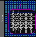
nanoFabric.
Compared to CMOS, CAEN-based devices have a higher defect density. Such
circuits will thus require built-in defect tolerance. A natural method of
handling defects is to first configure the nanoFabric for self-diagnosis
and then to implement the desired functionality by configuring around the
defects. Reconfigurabilty is thus integral to the operation of the
nanoFabric. Their nature makes nanoFabrics particularly well suited for
reconfigurable computing.
Motivation
Our research rests on the following premises:
- Electronic nanotechnology can build extremely dense and low power
computational elements.
- We will soon be able to manufacture devices with 1 billion logic
gates or even more.
- Conventional microarchitecture has problems handling the increasing
complexity of the designs.
The architecture we propose has better scaling properties than
CMOS-based devices, and will be able to smoothly take advantage of the
increasing number of hardware resources.
| Problem |
Solution |
| The verification and testing costs escalate
dramatically with each new hardware generation. |
The fixed computation core is a very large and homogeneous
reconfigurable fabric. Testing and verification for such a simple
device is trivial. We do not have a universal interpreter, which is
complex hardware structure (i.e., a CPU). |
| Manufacturing costs (both plant costs and non-recurring
engineering costs) have skyrocketed. |
The same masks are used to manufacture all the reconfigurable
devices; all complex processing is done in software,
post-fabrication. |
| The shrinking feature size will make the defect density
control very expensive; in the near future we will be unable to
manufacture large, defect-free integrated circuits. |
Reconfigurable hardware architecture can utilize substrates with
very high defect densities; the identical nature of the
computational elements makes possible the reconfiguration around the
fabric defects. |
| The dissipated power density (watts/mm2) of
state-of-the-art microprocessors has already reached values that
make air-cooling infeasible. |
We synthesize the program into a collection of small circuits,
only one of which is actively switching at any time moment. Thus
power consumption is dramatically reduced. |
| The clock frequency has increased to a value where global
signals across the entire chip are infeasible (the propagation delay
exceeds the clock cycle). Clock signal distribution often
takes more than 50% of the power consumption. |
We translate the program into a series of circuits which have
only local signals. Any remote communication is made using a
pipelined communication channel. Moreover, our circuits can be
implemented using asynchronous logic, which do not require a clock
signal at all. |
| The number of exceptions generated by the CAD tools
requiring manual intervention grows quickly with design
complexity. |
Placing and routing on a reconfigurable hardware substrate is
substantially simpler than handling CMOS. |
| Today's processors use extremely complicated hardware structures
to enable the exploitation of the instruction-level
parallelism (ILP) in large windows; however, the sustained
performance is rather low. |
The compiler synthesizes hardware tailored to each application;
the amount of parallelism exactly matches what the compiler can
extract. |
|


