CS 849C Lecture 2
First, a review of the matter from the last lecture, which focused on
computer architecture. The main ideas there were:
- Restoring logic, robust devices
- Parallelism (pipelining, superscalar, VLIW)
- Locality (memory hierarchies, caches)
Review of computer architecture
A simplified representation of the organization of a modern microprocessor
is shown in Figure 1. A simplified description of the components of a
modern microprocessor is that they consist of (1) Functional units
which perform the actual useful operations (2) Registers which
hold intermediate values between computations (3) Control logic
that ties together the operation of the various pieces and usually (4)
Cache memory which caches frequently used data so that costly
accesses to main memory are prevented for frequently used data.

The processor is interfaced to a memory that holds both instructions
and data, and it fetches instructions from memory and writes the
results back to memory, through a single interface. This organization of
processor, memory and interconnection is referred to as the von Neumann
(or Princeton) architecture. An alternative organisation is to have
separate program and data memory or separate program and data buses. This
is often referred to as the Harvard architecture.
The simplest technique for improving performance through hardware
parallelism is pipelining. Pipelining consists of breaking up the
operations to be performed into simpler independent operations, sort of
like the breaking up the operations of assembling a car in an assembly
line. A typical processor pipeline consists of 4 pipeline stages (1)
Instruction fetch, (2) Instruction decode (3) Instruction
execute and (4) Register file write-back/memory access. In
practice however, real architectures have many more physical pipeline
stages, with multiple physical stages corresponding to one of the above
stages. For example the execute stage might occupy 4 physical pipeline
stages
The primary advantages of pipelining are
- Parallelism
- Smaller cycles time
[smaller number of equivalent gates (FO4) per stage]
- Electrons don't have to go from memory to control to execute to
write back all in one cycle, they now just have to go from, say
control to register file or register file to exec, and they only have
to travel within the confines of one pipeline stage during each cycle.
There is however overhead in doing pipelining, both in terms of
performance (extra delay interfacing with pipeline latches) and area
(pipeline latches).
Caches are the other big thing done in the last 2 decades to improve
performance. Keep things locally if they are going to be used soon. From a
physics point of view, an access to memory which is almost exclusively off
chip, will mean signals have to travel that much further in one cycle. [In
practice, since we do not want to make the system as slow as its slowest
component (memory), and the cycle time is not determined by the memory
access time, and rather memory takes several cycles to complete].
Pipelining and caches are the big revolution in the last 20 years.
Caches are now on-chip. It is cheaper to be on chip, and there is a
tremendous amount of bandwidth, since we do not have to go out through
the processor pins, but rather all signals travel on the on-chip wires
which take advantage of device integration via photo-lithography.
In general to load from cache [first level cache] takes 1-2 cycles, and
to load from memory takes 50-500 cycles. If we have to wait 50 cycles,
then the whole pipeline stalls, and we loose a lot of the parallelism
we could have gotten from pipelining.
So we got parallelism from pipelining. Two other approaches are
Code example:
	a = (e << 3) + c;
	b = a + f;
	c = 5;
	d = n ^ 0xffff;
	e = n*n;
If we are going to execute them, the 3rd, 4th and 5th can be executed
independently of the first. In a superscalar processor, it exploits
what is called Instruction Level parallelism (ILP). It takes a bunch
of instructions and loads them all at once. These instructions are
taken out of a window of instructions, typically a window of about 16
instructions (issue window, reservation stations). Having a larger
window means we have a larger scope from which the processor will try
to find independent instructions, and execute them as soon as possible.
Now however, the register file gets much bigger (since we now need more
registers to be able to do more things in parallel).
Instructions are executed in parallel if they are independent. The neat
thing about superscalar architectures is that you take old program and
without re-compilation you can run faster without requiring extra effort
from the point of view of the programmer.
An other option is VLIW. Here, we do not try to do all the figuring
out on the fly in hardware. The processor is now a lot simpler, and the
complexity is moved to the compiler. Now instead of having 4 separate
instructions with dependences, the compiler arranges the program so that
the instructions sent to the processor are bundles (single instructions)
containing, say 4 independent operations, which are fetched at the same
time, and executed at the same time etc. The compiler now determines
what has to be done in parallel.
The difference between VLIW and superscalar:
Other types of parallelism:
- (Flynn classification, SIMD, MIMD, SISD, MISD)
- MIMD (message passing) these failed because they could not
scale with Moore's law, due to lots of custom hardware
- SIMD - one instruction, lots of data elements - e.g. have
an array and want to increment all the elements at once.
Very limited programming model
- Vector Processor - vector math add one vector (array) of data
to another vector (array) of data.
These architectures may not be sufficient to provide the
continued increases in performance that we have come to expect from
microprocessors. One of the reasons is process technology and the other
is economics. As we go to sub 100 nanometer technology, fabricating
these architectures in silicon becomes so much harder. For example,
in superscalar architectures with a large complex register file, we
now have wires that have to run a much larger length across the chip.
These lines at these small process dimensions begin to behave like
transmission lines as opposed to perfect conductors. They get slow
compared to transistors, and they do not scale as well as transistors.
The on-chip interconnect then begins to become a limit to performance.
Reconfigurable computing
The main idea: Take programs and run them thru a compiler. But instead
of getting a list of instructions, we get a circuit. Thus, into the
compiler goes our program and out of the compiler comes custom hardware.
Now, we would not like to just take that circuit and have it
implemented in silicon, because then as you might imagine, debugging
would be very expensive! Instead what is done is you take that circuit
description of your program and load it into a reconfigurable
fabric, like an FPGA or CPLD.
The way an FPGA works:
- Configuration for FPGA is held in a separate configuration
memory. Any function we desire can be implemented by storing
an appropriate configuration in the configuration memory, which
determines how the logic elements are wired up.

Now, going back to ILP. If we had a program with say 4 operations
that could be carried out in parallel, then when our
program is compiled to hardware, we have hardware to perform
each of those operations in parallel. Going back to the case
of the superscalar and VLIW machines, the hardware is fixed,
so if for example we had 2 functional units, then even though
our program has more ILP, we will not be able to exploit it.
Basically, in designing a general purpose processor, a tradeoff
is made by the designers as to how many functional units of different
types to include for the general case. For example on an architecture
we might have two integer ALUs, a shifter, a load-store unit,
an integer multiplier a floating point ALU. If there is some
application that would benefit significantly from having
4 integer ALUs and has no requirement for floating point hardware,
then there is nothing we can do, since the hardware is general (and fixed).
In reconfigurable hardware, rather than having to implement wires going to
memory etc, we could just map the output of one operations hardware
to the input of another. There are also many things that are
expensive to do in software but easy to do in hardware:
- Population count in software

- Bit reversal - just map the wires

- Custom bit-width hardware

- Have the hardware adapt to data input -- E.g. have custom
hardware generated for specific data inputs.

Nanofabrics paper
The primary message of the paper is that the method of putting these devices
together is different from photo-lithography,
and because of the inherently different nature of the technology,
we need a different architecture.
Question - how do you implement a memory cell ?
The architecture as it is described in the paper does not describe what
a memory cell will look like. What is done is when we want to store a
data value, e.g. a logic '1' then we configure the molecule on and vice
versa. To read data, we address the line, and read off the voltage at
the site. What is missing is how we can configure these devices on/off
quickly, and how do we access the multiplexers to address the data.
The reason why this is hard is that the wires are e.g. 10nm apart, but
now how do we address an individual wire ? one way would be to have some
kind of a multiplexer, taking in log(n) wires and having n wires out, with
incoming control lines. So we would go from fat wires to nanoscale. The
multiplexers would have to be 10x bigger than a nanoblock. So rather we
address the wires in the time domain. A method that will be difficult to get
right (because of the need for precise process controls) is as follows:
- Given the logic array if you look at the diagram for the
nanoblock in Figure 2 below each one of the hashed regions is
implemented with photo-lithography, and we want to minimize the
number of these per nanoblock because the photo-lithography
has rules and restriction on how close we can put these
photo-lithographically made blocks together, like a 'cheap' 100nm
process, so we are getting say 1.4um on the side of a nanoblock
if we want to have 7 of these per side. Imagine the red wire
is a big resistor. we run a high voltage between the 2 nodes
to configure it. The way to get the high voltage across it,
say 10V, we put 5 volts on one side and -5 volts on the other
side, so there is a gradient of voltage across the wire, and
there is only one position that has +10V. So we start off with a
very high voltage, applied to the entire array. and slowly turn
voltage and leave behind those that we want to program, thus
using time multiplexing as opposed to space multiplexing. This
approach does not work. One of the reasons is that you have to
get the process tolerances just right.

The wires are made of carbon nanotubes which are essentially single
molecules about 1.2 nm in diameter. They have a conductivity of the square
of the conductivity of copper, at the nanometer scale. With copper at
that small dimension we get into grain size issues etc.
Molecular Switches
The currently proposed molecules for molecular switches are made of rotaxane

If the ring (orange in Figure) moves to the right, the switch is closed
and if the ring is to the left, it is open.
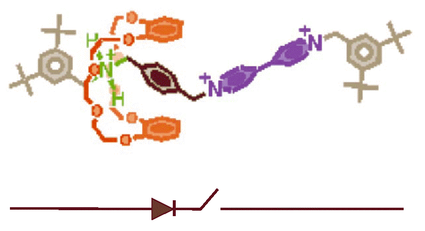
 FPGAs require a separate configuration memory. We have all these
extra wires from the memory cells with of the order of 10-100x
overhead. With the reconfigurable molecular switch on the other hand,
the memory/state is where the ring is, so it holds its own state and
we can also program it with the same wires we use to read data.
FPGAs require a separate configuration memory. We have all these
extra wires from the memory cells with of the order of 10-100x
overhead. With the reconfigurable molecular switch on the other hand,
the memory/state is where the ring is, so it holds its own state and
we can also program it with the same wires we use to read data.
We use electricity to cause a conformational change in the molecule
(movement of the ring). This programming does not happen quickly, as it
involves molecular changes. Though current molecular electronic devices
may seem a little primitive, technologies for fabricating these molecular
electronic devices are constantly improving.
A big issue however, is the contact resistance between the nanoscale and
the photo-lithographically fabricated devices. It is of the order of a
giga-Ohm and tera-Ohm. Creating a truly ohmic contact is hard. There have
been some claims to success in this, but do not know of any published
results.
The NanoFabric architecture
Nanoscale devices must still interface with the outside world, which is
dominated by photo-lithographically manufactured devices. Even within
a nanotech-based device, the device dimensions are restricted by the
minimum feature sizes at the micro-scale.
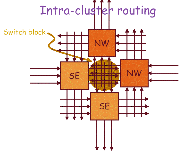
SE block

Input and outputs are nanoscale wires. It is easy to have the wires cross,
but rather difficult to connect them end-to-end, inputs on one side and
outputs on the other side. To make connections between blocks, we float
in the nanoblocks and get them to settle into pits in a substrate. Same
thing happens for the NW blocks. There is a reasonable amount of slop
in how accurate the placement of each nanoblock is, as can be seen from
the Figure below.
The wires are probably originally coated, and after we do the float,
we do a dissolve step. This would make it possible to have some coating
to prevent the wires from breaking during the floating in.
In connecting nanoblocks, there is restriction on which blocks can be
interconnected. Due to the arrangement of inputs and outputs and the
alignment of nanoblocks, each SE block can only send outputs to the NW
block to its upper right hand, and to the SE block to its lower left.
All other communications will therefore be going through intermediate
SE and NW blocks.
Is this layout sufficient to map any circuit onto it (as we can do
for FPGAs as previously mentioned) ? We can think of this layout as
a 2-dimensional mesh. It will takes 4 hops to get across, which slows
communication form A to B down by a factor of 4.
Defect Tolerance
When making a complex irregular structure, just take out one piece and
the whole thing is broken. If you have regularity in the underlying
structure, then we can program around the defects.
Imagine you are programming your MLA to implement a half-adder, we can do
things to avoid the defect. Finding the defects is however hard, since
we cannot go in and address independent wires. The general approach is
that you test enough of it externally, so that it can then test itself.
Since we cant go in a look in at any individual element, what is instead
done is we for example implement a Linear Feedback Shift Register (LFSR)
on the fabric. The LFSR is essentially a pseudo-random number generator,
that will generate a known sequence of pseudo random outputs. Several
LFSRs are implemented in the grid in the fashion shown in the figure
[insert figure from notes]. Now, we crank each of these LFSRs that are
mapped on different (though overlapping) parts of the fabric and check
the results. If there is a defect in any part of the fabric onto which
an LFSR is mapped, the generated outputs will begin to diverge from the
correct sequence. So using the outputs from the diffenrt LFSRs mapped
to the fabric, we can narrow down on which are contains the defect.